
A team of scientists at the Tokyo University of Science has developed an artificial intelligence-based technique that can automatically identify material properties from X-ray absorption spectroscopy (XAS) data, a breakthrough that could accelerate the design of new materials used in semiconductors, batteries, and catalysts.
The research, led by Professor Masato Kotsugi alongside Ms Reika Hasegawa and Dr Arpita Varadwaj, introduces a machine learning framework capable of interpreting complex XAS data without the need for extensive human expertise. Their findings were published in Scientific Reports.
XAS is a widely used technique to probe the electronic and atomic structures of materials, but its analysis has traditionally required expert interpretation and time-consuming manual work. The method developed by the Tokyo team applies dimensionality-reduction algorithms to simplify and classify large spectral datasets, allowing the system to distinguish between different atomic structures and defects in materials.
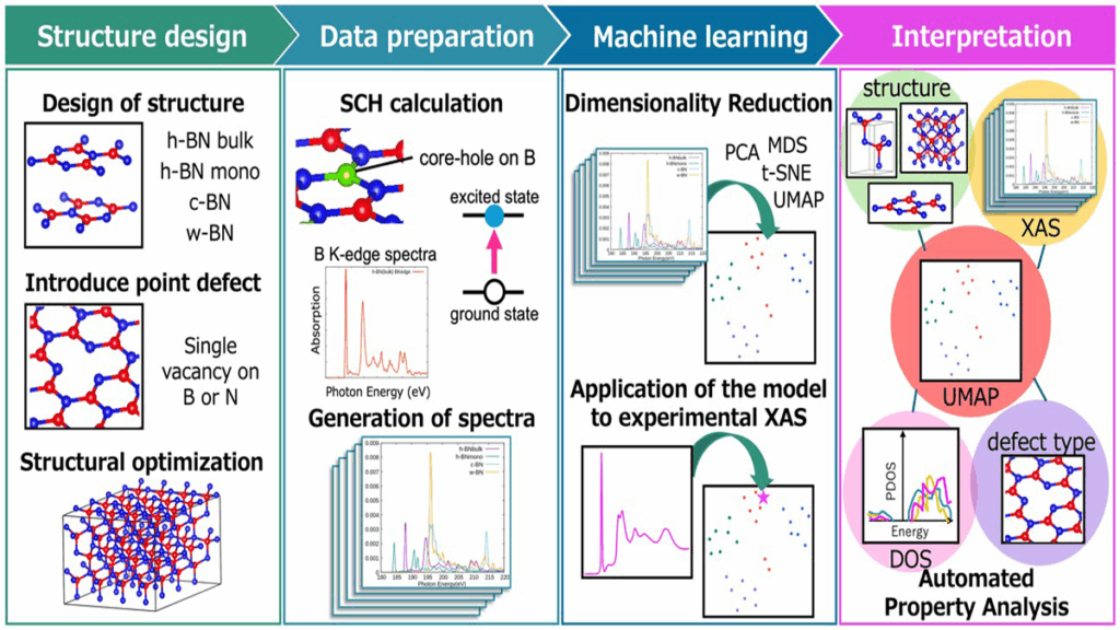
Among several machine learning models tested—including Principal Component Analysis, Multidimensional Scaling, and t-distributed Stochastic Neighbour Embedding—the researchers found that the Uniform Manifold Approximation and Projection (UMAP) algorithm produced the most accurate and robust results. It was able to identify subtle differences in electronic structures even in noisy experimental data, outperforming earlier statistical approaches.
“Our findings show that UMAP can be a valuable tool for rapid, scalable, and objective material identification using complex experimental spectral data,” said Prof Kotsugi. He added that the method “demonstrates the potential of autonomous structural identification, opening up new possibilities for data-driven material design.”
The team generated and validated XAS data for three phases of boron nitride—an important compound used in semiconductors and energy devices—using both theoretical and experimental methods. Their AI-driven analysis achieved higher accuracy than previous techniques while revealing previously hidden variations in the materials’ electronic states.
The researchers plan to implement the system at Japan’s Nano-Terasu synchrotron radiation centre, where it could be used to analyse large volumes of experimental data in real time. They expect the technology to speed up the discovery and optimisation of functional materials across a range of industries.
There’s plenty of other editorial on our sister site, Electronic Specifier! Or you can always join in the conversation by visiting our LinkedIn page.