Specialising in software simulation tools, Ansys provides its customers with the ability to test designs ranging from semiconductor products to 5G communication systems, to “accelerate time to market and reduce risk in developing complex communication systems,” according to Jayraj Nair, Field CTO for Hi-Tech and APAC Region, Ansys in an exclusive interview with IoT Insider.
Ansys’ advanced engineering simulation tools enable the virtual testing of product designs, and are used across an array of industries, including aerospace, automotive, and electronics.

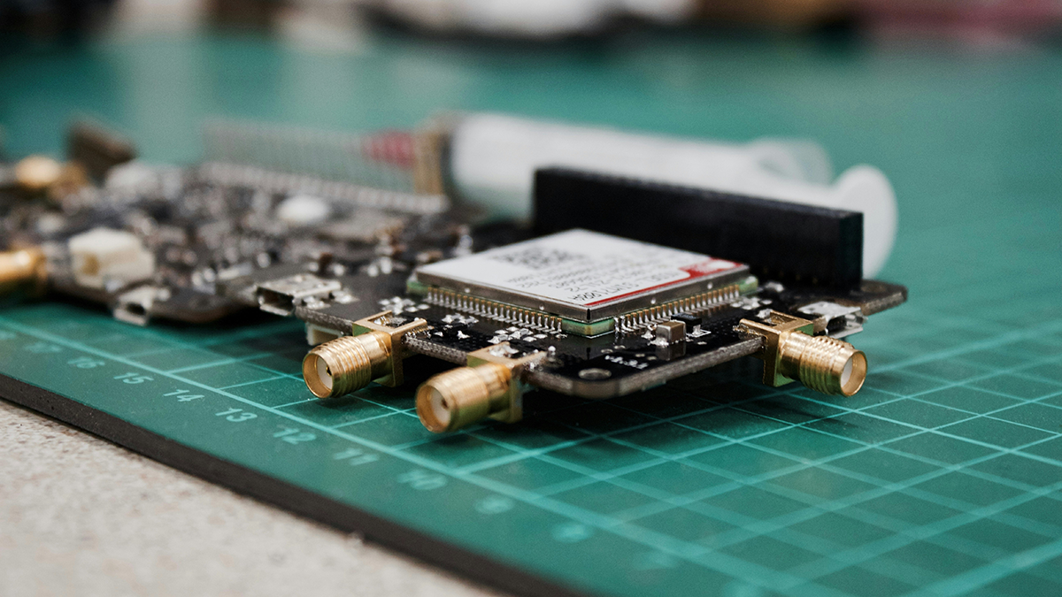
The boom in 5G deployments represented growth not seen before with 3G and 4G systems, as companies saw in 5G a cellular technology that would provide high speeds, low latency and reliable connectivity. According to analysis provided by 5G Americas in March 2025, 5G connections reached 2.25 billion worldwide; expanding four times faster than 4G in a comparable period.
The complexity of 5G system design, however, means simulation tools play an important role in allowing companies to evaluate the system architecture and its performance before they deploy it – meaning they can avoid the expense associated with physical prototyping and field testing.
This is where Ansys operates. As Nair put it: “Simulation provides the ability to explore, validate, and optimise complex systems before committing to expensive prototypes … Our tools enable engineers to assess antenna placement, mitigate interference, ensure thermal stability, and optimise power delivery.”
Some of the challenges its customers face in developing 5G communication systems include exactly that: power integrity, thermal management, and high-speed signal integrity.
“These are particularly pressing in dense 5G base stations and mobile devices where compact form factors and increased bandwidth push the limits of conventional design methods,” noted Nair. “Simulation is proving indispensable in addressing these challenges early [on] in the design cycle.”
Because 5G systems operate at higher frequencies, with “tighter power margins and greater thermal demands,” Ansys responds to these requirements with co-simulation frameworks that can perform bidirectional coupling of physical efforts – in other words, they can provide realistic system behaviour under actual operating conditions.
Semiconductor trends
5G isn’t the only industry in which its growth and development is presenting unique design challenges; in semiconductors, for instance, the growing number of transistors and integration of NPUs, GPUs and CPUs on chips are affecting customers’ simulation needs.
Moore’s Law, which stipulates that the number of transistors on a chip will double every year and result in increased computing power, is potentially reaching its limits due to a number of factors. This includes the size constraints of a chip, the cost of manufacturing process nodes, and diminishing returns. However, companies are seeking to circumnavigate this through processes such as 3D chip stacking as the dawn of the AI era demands more computing power from semiconductors.
All of this means Ansys’ customers rely on simulation tools to model the chips they are creating in order to understand performance.
“Traditional single domain tools can’t keep up,” added Nair. “Customers need scalable, multi-domain simulation platforms that can span from nanometre scale devices to full system level behaviour.”
Trends that are expected to put the pressure on designing chips include chiplet architectures; co-packaged optics; and AI workload demands.
“These trends bring tight thermal constraints, complex power delivery requirements, and electromagnetic interference issues that can’t be resolved with traditional tools,” said Nair. “The need for system-level co simulation, multi-scale modelling, and AI-enhanced design is only going to intensify.”
This is already happening: Siemens, as one example, has a software portfolio that provides predictive engineering and support assistance powered by AI, designed to enable engineers to streamline workflows. In recent news, it announced that it would make its technology more accessible to small and medium-sized businesses (SMBs) in a move to “democratise” PCB design.
Ansys are already using AI in their own tools, along with machine learning (ML). In one example, “ML helps reduce simulation runtimes by using surrogate models trained on high-fidelity data, allowing engineers to explore design spaces more quickly”.
Looking ahead, the big talking points for Ansys will be to expand the role of simulation in heterogeneous computing, sustainability-driven design, and AI-accelerated engineering.
“The semiconductor industry is undergoing a transformation, not just technologically but also in how we train and equip our workforce,” Nair concluded. “Simulation is no longer just a verification step; it’s become a catalyst for innovation.”
There’s plenty of other editorial on our sister site, Electronic Specifier! Or you can always join in the conversation by commenting below or visiting our LinkedIn page.