
This piece from NGK INSULATORS (NGK) covers its plans for electronica 2022 and the exciting technology that will be on display at its exhibition stand.
NGK had previously only participated in electronica online, but this year, it will participate onsite for the first time throughout the event, which runs from the 15th to the 18th of November 2022.
At the booth, NGK’s solar-powered indoor/outdoor position tracker will be exhibited for the first time. An NGK employee will host a lecture about EnerCera, a battery for IoT devices (more on this below), at the event hall on the 16th of November.
electronica, which has been held in Munich, Germany for nearly half a century since the first event in 1964, is the industry’s leading comprehensive trade fair for electronic components where the latest technology and products related to electronic components are displayed.
The theme of NGK’s exhibition will be ‘Making smart society more comfortable by contributing to digital society with ceramic technology’. As covered in the following subsections, the exhibit will feature EnerCera, a battery for IoT devices that contributes to the realisation of Society 5.0; a GaN (gallium nitride) wafer that improves the performance of RF devices and high-power devices; and bonded wafers (dissimilar material bonded wafers), which contribute to the production of highly functional semiconductors and electronic components.
NGK will also display a variety of ceramic products for electronic devices which harness its unique ceramic technology, including translucent alumina ceramic wafers which possess the properties of translucency and high modulus of rigidity, and capacitance sensors, which make it possible to detect the conductivity or concentration of various chemical solutions.
Three NGK technologies to be showcased at electronica
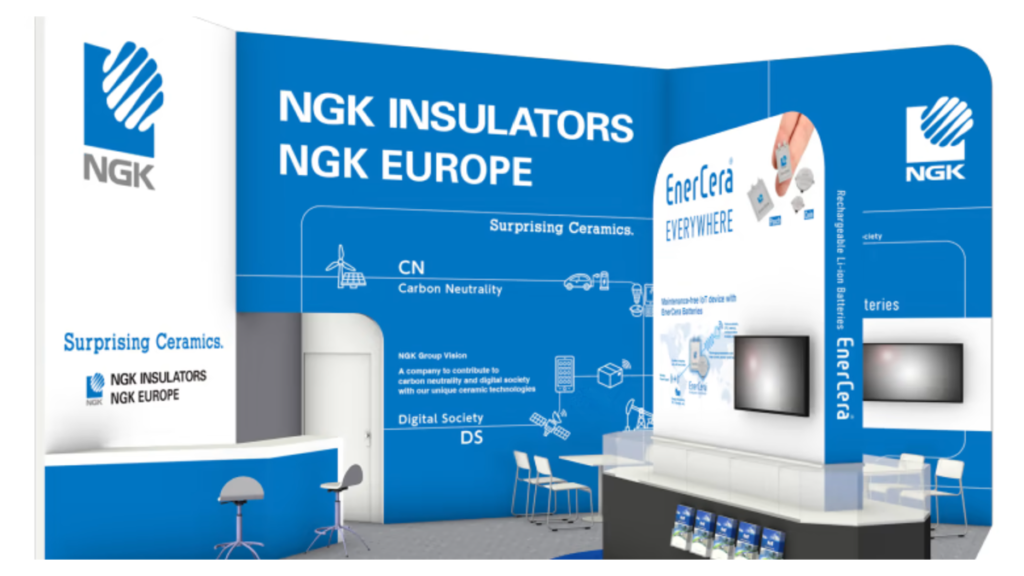
EnerCera, a power supply for IoT devices
The ultra-thin and compact lithium-ion rechargeable battery EnerCera is highly heat resistant, being able to withstand temperatures of 105°C. It is highly durable due to the use of ceramic electrodes, and can be used as a backup power supply for devices and sensors that operate in harsh environments such as factory automation (or FA) and plants.
EnerCera is characterised by its ability to store even small amounts of electricity due to its low internal resistance. Combined with power supply technologies such as solar power generation and wireless power transfer, EnerCera enables independent IoT devices such as position trackers for logistics to be used for long periods of time.
On top of this, because EnerCera is ultra-thin and compact, it can even be used in wearable devices, and will help visualise the flow of factory workers and others and reduce manpower by improving operations.
At the booth, NGK will introduce examples of application through videos and augmented reality exhibits through which visitors can experience specific usage scenarios of standalone IoT devices that utilise EnerCera. (For the first time, NGK will also showcase its indoor/outdoor position tracker developed in collaboration with Exeger Operations AB, TACHIBANA ELECTRONIC SOLUTIONS, and Semtech Corporation.) The combination of EnerCera eliminates the need for battery replacement and recharging work required with conventional trackers, making the system maintenance-free.
GaN (gallium nitride) wafers
GaN wafers exhibits low defect density through NGK’s proprietary liquid phase crystal growth method in comparison to the conventional vapor phase crystal growth method. At the booth, NGK will display conductive GaN wafers and semi-insulating GaN wafers. Conductive GaN wafers realise ultra-bright laser diodes and power devices with high power levels and low levels of loss.
Semi-insulating GaN wafers improve the performance of RF devices for 5G and 6G wireless communication base stations, various radars, and satellite communications, which all require higher frequencies and higher output.
Bonded wafers (dissimilar material bonded wafers)
Bonded wafers are realised by techniques of bonding dissimilar materials and high-precision polishing. Combinations of dissimilar materials make it possible for bonded wafers to deliver performance and functionality beyond wafers made from a single material, such as suppressing thermal expansion, ensuring mechanical strength, and enhancing thermal conductivity. They are notable for enabling a choice of material matched to the usage, such as semiconductor and piezoelectric crystal for the functional layer, and silicon, sapphire, crystal, or glass for the base material.
Sintered-PZT bonded wafers will be displayed at the booth. Sintered-PZT bonded wafers are fabricated through a sintering method applied to PZT, a piezoelectric material which can be deformed when electricity is applied and generate electricity when deformed. They are bonded to a base material and polished for use as a functional layer and applied to wireless speakers and sensors for applications such as autonomous driving.
More information on major events like electronica can be found at our page on ‘events news’ here.
Plus, you can learn more about breakthroughs in manufacturing at our Industrial page. And to delve deeper into our content, you can comment below or visit our LinkedIn page and sister site, Electronic Specifier!