Programmable integrated circuits are small electronic components constructed in such a way that a designer can configure them to perform a specific function. These programmable logic devices range in complexity from a few hundred to tens of thousands of equivalent gates. Outlining types of programmable integrated circuits (ICs), their main functionality, similarities, and differences, this article will explore the pros and cons of each type and examine the fields of their applications.
Programmable IC families
Since the dawn of electronics, engineers tried to create their circuits as versatile as possible to save time, resources, and a budget. With the rise of ICs invented by Robert Noyce at Fairchild Semiconductor in 1959, this task became more substantial than ever. The more applications your IC can cover, the more pieces you can supply to customers, and the more profit your business makes. That resulted in a relatively simple internal IC design. In this way, it could be used in a variety of circuits but at the cost of using many external components. Often levelling the advantage of miniaturisation. That all changed with the invention of the microcontroller (MCU) in 1971 by two engineers at Texas Instruments Gary Boone and Michael Cochran. Now one tiny chip could be used in a previously unimaginable variety of applications thanks to its programmability. In a short period after that, more and more types of programmable ICs began to appear, each with its unique functions and use cases.
- MCU (Microcontroller) is a compact integrated circuit designed to govern a specific operation in an embedded system. A typical microcontroller includes a processor, memory, and input/output (I/O) peripherals on a single chip.
- PSoC (programmable system on a chip) is a family of microcontroller integrated circuits by Infineon. These chips include a CPU core and mixed-signal arrays of configurable integrated analog and digital peripherals.
- FPGAs (field programmable gate arrays) are semiconductor devices that are based around a matrix of configurable logic blocks (CLBs) connected via programmable interconnects. FPGAs can be reprogrammed to desired application or functionality requirements after manufacturing.
- CPLD (complex programmable logic device) is a programmable logic device with complexity between Programmable Array Logic (PAL) and FPGA, and architectural features of both. The main building block of the CPLD is a macrocell, which contains logic implementing disjunctive normal form expressions and more specialised logic operations.
- Programmable analog ICs (PAsICs) are integrated circuits that offer configurable analog functionality, allowing users to customise and adjust analog circuitry based on specific application requirements. PAsICs provide flexibility in analog signal processing by enabling the programming or reconfiguration of various analog functions, such as amplifiers, filters, voltage references, and other analog components. These ICs typically allow for adjustments in analog parameters through programming rather than requiring physical modifications, offering versatility and adaptability in various electronic systems and applications.
- GreenPAK programmable mixed-signal matrices provide a small and low-power component for commonly used mixed-signal functions. The circuit design can be created by programming the One Time Programmable (OTP) Non-Volatile Memory (NVM) to configure the interconnect logic, the IO pins, and the macrocells. These highly versatile devices allow a wide variety of mixed-signal functions to be designed within a very small and low-power single-integrated circuit. Their usage has grown dramatically with the increased use of cell phones, telecommunications, portable electronics, and automobiles with electronics and digital sensors.
Programmable ICs comparison summary
See the table below for the pros and cons of each type.
Table 1. Programmable ICs comparison
| Criteria | Microcontrollers (MCUs) | PSoCs | FPGAs | CPLDs | PAsICs | Mixed-signal programmable Matrices (GreenPAKs) |
| Advantages | ||||||
| Cost-effectiveness | ?? | ?? | ||||
| Low power consumption | ?? | ?? | ?? | |||
| Integrated peripherals | ?? | ?? | ?? | |||
| Mixed-signal integration | ?? | ?? | ?? | |||
| High customisability | ?? | ?? | ?? | ?? | ||
| Parallel processing | ?? | ?? | ||||
| Flexibility | ?? | ?? | ||||
| Customisability | ?? | ?? | ?? | ?? | ||
| Low power consumption (in CPLDs) | ?? | ?? | ||||
| Custom analogue functionality | ?? | ?? | ||||
| Integration | ?? | ?? | ?? | ?? | ||
| Reconfigurability | ?? | ?? | ?? | ?? | ||
| Zero-code programmability | ?? | ?? | ||||
| Disadvantages | ||||||
| Limited processing power | ?? | ?? | ?? | |||
| Limited customisability | ?? | ?? | ?? | |||
| Limited parallel processing | ?? | ?? | ||||
| Complexity | ?? | ?? | ||||
| Power consumption | ?? | ?? | ||||
| Higher cost | ?? | |||||
| Specificity | ?? | ?? | ||||
| Complex design | ?? | ?? | ||||
| Requires programming skills | ?? | ?? | ?? | ?? |
As we can see, Mixed-signal programmable Matrices are absolute winners according to the table. However, they are not the solution for every circuit design and cannot compete as equals with the FPGAs, for instance. Nevertheless, this broad IC family can be the next best alternative. An example of these types of ICs is a GreenPAK family of cost-effective NVM programmable devices.
Why GreenPAK?
GreenPAK’s integrate analog components, such as operational amplifiers (OPAMPs), analog comparators (ACMPs), analog-to-digital converters (ADCs), digital-to-analogue converters (DACs), and programmable interconnects, with highly configurable digital logic blocks such as clocks, LUTs, DFFs, counter/delays, memory, etc. In most cases, GreenPAKs can be considered as a PSoC without a microcontroller core, although some of them contain digital logic blocks that can perform rudimental math.
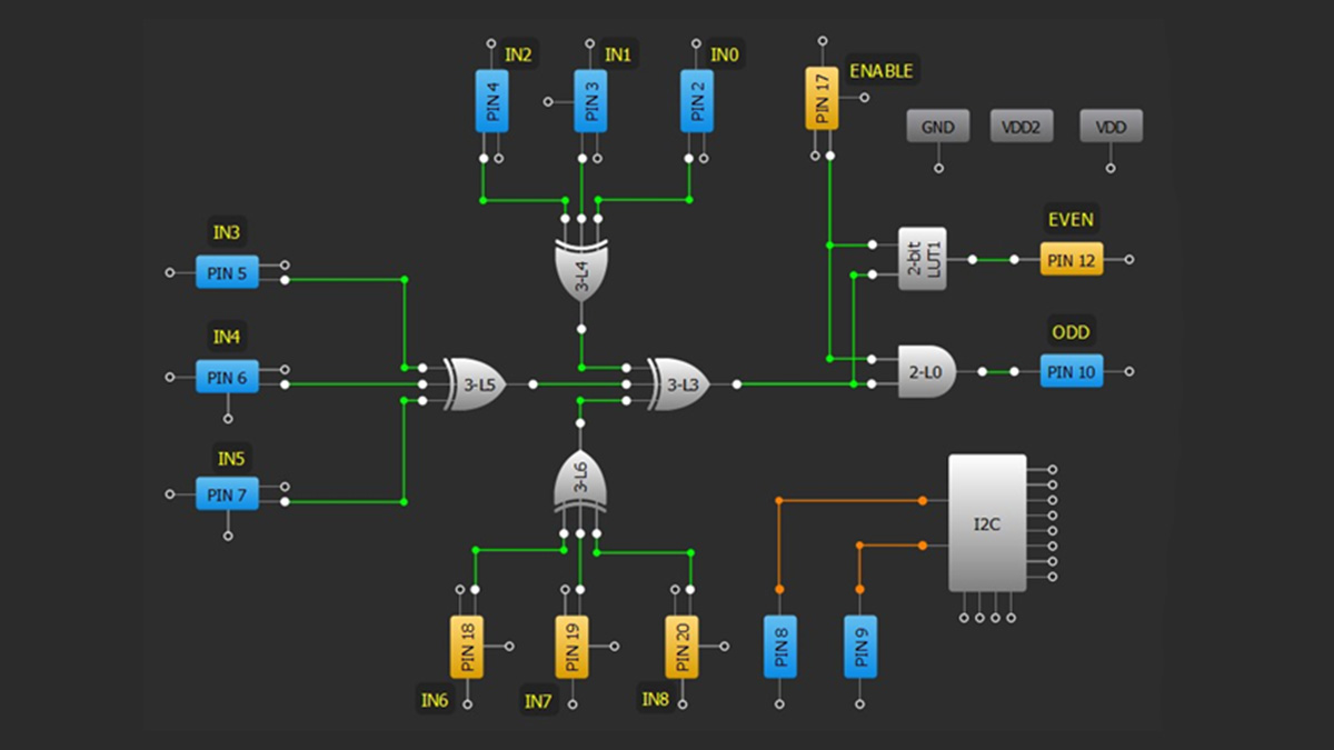
These devices allow users to configure both analog and digital functions, enabling the processing of mixed-signal inputs. They can perform analog signal conditioning, digital signal processing, and mixed-signal interfacing tasks. Also, thanks to its highly intuitive software it takes just minutes to start working on a new design instead of spending hours, sometimes days, learning new software documentation, or in the worst case a new programming language. The GreenPAK ICs are zero-code programming devices, meaning no programming language is required to configure the IC. All configuration is done via the graphic interface demonstrated in Figure 1.
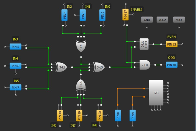
Figure 1: Go configure example project
See also the GreenPAK Cookbook. This document is designed for electronics design engineers to highlight where a GreenPAK can be used within their projects. It outlines different techniques and provides complete applications to help designers use GreenPAK on their own.
GreenPAKs find applications in systems where both analog and digital signals need to be processed, such as in communication systems, sensor interfaces, data acquisition systems, and audio processing devices. They are valuable in applications that require precise conversion, filtering, and manipulation of signals in real time. The full library of real-life applications designed using GreenPAK can be found at Renesas’ website.
These mixed-signal programmable matrices offer a bridge between the analog and digital worlds, providing a comprehensive solution for applications that demand sophisticated processing capabilities for both signal types. Their flexibility and configurability make them suitable for a wide range of applications where precise control over mixed-signal processing is crucial such as IoT.
Every type of programmable IC described in Table 1 has its own advantages, unique functions, and use cases. However, what makes GreenPAKs unique is their extreme versatility and cost-effectiveness. This means one device family can satisfy almost all design needs, and in many cases replace all the ICs listed above. Simultaneously, it is power and PCB space efficient. Consuming nano amperes when idle in a tiny STQFN package. This kind of versatility is often used to considerably reduce PCB size, BOM cost, and design time. See the design optimisation example in Figure 2.
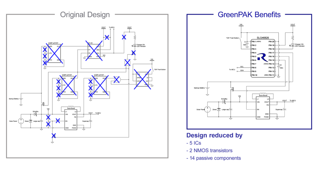
Figure 2: Design optimisation example
Very often circuit design engineers design their devices or parts of them motivated not by cost, PCB space, or current consumption effectiveness, but by a combination of laziness and lack of knowledge of the IC market.This is understandable, given there are many IC companies offering all sorts of ICs for every solution. It would take a lifetime to learn all of them. So, the average engineer, for example, may pick one MCU or family of MCUs and puts it into every design avoiding learning new documentation for any new IC. Moreover, each company has its own software, and sometimes even programming language. This can result in inefficient and overkill designs, such as using an MCU to blink an LED. While this may justify a decrease in man-hours, it results in a competitive disadvantage overall. This is where the GreenPAK family proves invaluable, especially in Internet of Things (IoT) applications.
GreenPAK in IoT
Integrated Circuits used in IoT must meet specific requirements to enable efficient and reliable functionality within devices. These requirements are shaped by the diverse nature of IoT applications, which can range from small sensors to complex data processing systems. Here are some key requirements for ICs used in IoT and how GreenPAKs comply with them:
- Low power consumption: IoT devices are often battery-powered or need to operate on low power to extend their lifespan. All the ICs within the GreenPAK family are very energy-efficient, enabling devices to operate for extended periods without frequent battery replacements. Typical idle current consumption is less than 1 µA.
- Small form factor: IoT devices are often compact and portable. All GreenPAKs come in tiny TQFN and MSTQFN packages, the smallest of them is 1.0 x 1.2 x 0.55 mm in size allowing it to easily fit within the limited space of any IoT device.
- Low cost: IoT applications often involve mass deployment of devices. Cost-effective ICs are essential to keep the overall cost of IoT devices affordable. The price for GreenPAKs starts at $0.18.
- Security features: IoT devices are vulnerable to security threats. Since GreenPAKs do not have CPU cores, they are impossible to hack into.
- Sensors and actuators integration: IoT devices often require sensors (e.g., temperature, humidity, motion) and actuators (e.g., motors, relays) for data collection and control. The Broad GreenPAK family includes ICs with all sorts of input and output interfaces. From analog comparators, OPAMPs, and ADCs on the input to DACs and high-power full half/bridges on the output, to name a few.
- Processing power: Depending on the complexity of the IoT application, ICs should provide sufficient processing power to handle data processing tasks, especially for edge computing and real-time analytics. GreenPAKs incorporate the wake and sleep timer which can further reduce their power consumption as well as the power consumption of other ICs within the IoT device.
- Low latency: Some IoT applications, particularly those involving real-time control or monitoring, require low-latency communication. GreenPAKs used for such applications have signal propagation delays of tens of nanoseconds only.
- Compatibility and interoperability: GreenPAKs are designed to work seamlessly with other components and protocols, ensuring compatibility and interoperability within the IoT ecosystem.
- Ease of programming and development: The GreenPAKs ecosystem includes user-friendly development tools and zero-code software with a highly intuitive GUI that allows the creation of custom ICs within minutes, facilitates the development of IoT applications, and reduces time-to-market.
- Environmental durability: IoT devices can be deployed in various environments, including outdoors and industrial settings. The GreenPAK family includes ICs designed to withstand environmental factors such as temperature variations, humidity, and vibration. Including ICs with extended operating temperature range -40°C to 125°C and automotive AEC-Q100 qualified ones.
Meeting these requirements ensures that GreenPAKs used in IoT applications can enable reliable, energy-efficient, and secure connectivity and data processing, making them suitable for but not limited to the diverse range of IoT devices and deployments.
Conclusion
The GreenPAK IC family from Renesas Electronics Corporation is a standout solution not only for IoT but also for handheld, home appliances, automotive, and other end applications. For further insights and guidance, there is a great collection of application notes on the Renesas’ website.

Nazar Sliunchenko is Technical Documentation Manager at Renesas Electronics.